![\includegraphics[width=0.7\textwidth]{SL_scheme}](img84.gif) |
Semiconductor superlattices consist of an alternating layer sequence
of two different materials. At sufficient barrier thickness
electrons are assumed to be localized in the individual wells.
The resulting schematic energy band structure is shown in
Fig. 9. Furthermore it is assumed, that electrons in one well are in local equilibrium
with the majority of them occupying the lowest energy level. Electrons can tunnel
from the ground state of a well to a free state of the next well, where a possible difference
between the state energies can be compensated by the electric field acting between
neighbouring wells.
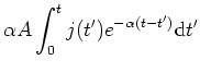
The current density
![]() from well
from well ![]() to
to
![]() is thus a nonlinear function of the electric field
is thus a nonlinear function of the electric field ![]() between the two wells as well as of the electron densities
between the two wells as well as of the electron densities ![]() and
and ![]() in the involved wells. For concrete microscopic calculations
of
in the involved wells. For concrete microscopic calculations
of
![]() we have used the sequential tunneling model which
has been developed in our group, cf. review paper by A. Wacker [17].
For the contact currents at the emitter
we have used the sequential tunneling model which
has been developed in our group, cf. review paper by A. Wacker [17].
For the contact currents at the emitter
![]() and
the collector
and
the collector
![]() we simply assume Ohmic
boundary conditions, which are characterized by a contact conductivity
we simply assume Ohmic
boundary conditions, which are characterized by a contact conductivity
![]() .
.
![]() is the number of quantum wells in the superlattice.
is the number of quantum wells in the superlattice.
Therefore the following equations of motion for the
electron densities arise:
![\includegraphics[width=0.5\textwidth]{ama02a_fig4}](img109.gif) |
![\includegraphics[width=0.5\textwidth]{ama02a_fig2a}](img110.gif) |
Depending on the physical parameters (especially on ![]() and
and ![]() ) the system of equations (10), (11)
and (12) at a constant
) the system of equations (10), (11)
and (12) at a constant ![]() has either stationary or oscillatory
spatially inhomogeneus solutions (field domains bounded by
electron accumulation and depletion).
In the stationary case the system is in
general multistable, i.e. for one value of the voltage there are many stable
branches, which differ for instance, in the resulting current. In collaboration with L. Bonilla (Madrid),
the next question to be treated was which of these branches would be selected by the system after an
abrupt or continuous change of the external voltage [9,36]. At this point we determined
that the final state
of the system can depend very sensitively
on the difference between the initial and final voltage. This property
could then be used to select operating points.
The majority of the partially surprising effects could be explained
by the fact that at the emitter, pairs of electron accumulation and depletion
fronts (dipole) were generated. Our theoretical predictions on switching dynamics
between multistable states were
later quantitatively confirmed by experiments performed at the
Paul-Drude-Institute in Berlin [5].
has either stationary or oscillatory
spatially inhomogeneus solutions (field domains bounded by
electron accumulation and depletion).
In the stationary case the system is in
general multistable, i.e. for one value of the voltage there are many stable
branches, which differ for instance, in the resulting current. In collaboration with L. Bonilla (Madrid),
the next question to be treated was which of these branches would be selected by the system after an
abrupt or continuous change of the external voltage [9,36]. At this point we determined
that the final state
of the system can depend very sensitively
on the difference between the initial and final voltage. This property
could then be used to select operating points.
The majority of the partially surprising effects could be explained
by the fact that at the emitter, pairs of electron accumulation and depletion
fronts (dipole) were generated. Our theoretical predictions on switching dynamics
between multistable states were
later quantitatively confirmed by experiments performed at the
Paul-Drude-Institute in Berlin [5].
By closer investigations on the front generation process at the emitter,
as well as of the motion of the fronts inside the device, we successfully generated
complex self-oscillations like tripole modes [19].
It was shown that the front generation at the emitter
depends substantially on the contact conductivity ![]() and the total current
and the total current ![]() .
In particular, chaotic front dynamics in a non driven superlattice
were proven for the first time [18]. A typical bifurcation scenario is shown
in the electron density plots in
Fig. 10. We can see that with increasing voltage the superlattice
exhibits both periodic and chaotic behaviour. The full bifurcation diagram (Fig. 2.11)
exhibits an alternating sequence of chaotic and periodic regions as well as a striking
cobweb structure, whose center lies at
.
In particular, chaotic front dynamics in a non driven superlattice
were proven for the first time [18]. A typical bifurcation scenario is shown
in the electron density plots in
Fig. 10. We can see that with increasing voltage the superlattice
exhibits both periodic and chaotic behaviour. The full bifurcation diagram (Fig. 2.11)
exhibits an alternating sequence of chaotic and periodic regions as well as a striking
cobweb structure, whose center lies at ![]() .
.
Our further objective was to reduce the front model to a simple elementary basis.
In collaboration with the group of U. Parlitz (Göttingen) we found a surprising analogy to a tank
model, which is normally used in a totally different context, for describing industrial production
processes [28]. Consider a system of a given number of tanks.
A swithching server fills one of the tanks and at the same time
all nonempty tanks drain. The server then switches to a new tank, as soon as
it is empty, under the condition that the tank which it is currently filling
has reached the minimum filling height ![]() . The relation
between the inflow- and outflow rates is chosen such, that
the total amount of the water
. The relation
between the inflow- and outflow rates is chosen such, that
the total amount of the water ![]() stays constant. The filling heights
of the tanks correspond to the length of the high-field domain (in the superlattice system)
between a depletion and an accumulation front or between the
first depletion front and the emitter for the tank that is actually being
filled. The switching of the server in the tank system coresponds to the
generation of a dipole front at the emitter in the superlattice system.
stays constant. The filling heights
of the tanks correspond to the length of the high-field domain (in the superlattice system)
between a depletion and an accumulation front or between the
first depletion front and the emitter for the tank that is actually being
filled. The switching of the server in the tank system coresponds to the
generation of a dipole front at the emitter in the superlattice system.
![\includegraphics[width=0.5\textwidth]{ama03_fig4}](img114.gif) |
For three tanks the resulting dynamics is described by a one dimensional piecewise linear
iterated map as in the inset of
Fig. 12. This modified map
has only one bifurcation parameter ![]() . The corresponding
bifurcation diagram in Fig. 12 agrees in detail with the microscopically calculated
bifurcation diagram in
Fig. 11. In particular the cobweb structure
is reproduced in detail. We can therefore show that the front dynamics in the superlattice
can be explained on a very fundamental basis using iterated maps [28].
Because the microscopic properties of the superlattice do not come up, it must be assumed, that a
similar reduction may also be possible
for complex front systems with global coupling
in many other disciplines, and that our reduced model may describe a universal
bifurcation scenario.
. The corresponding
bifurcation diagram in Fig. 12 agrees in detail with the microscopically calculated
bifurcation diagram in
Fig. 11. In particular the cobweb structure
is reproduced in detail. We can therefore show that the front dynamics in the superlattice
can be explained on a very fundamental basis using iterated maps [28].
Because the microscopic properties of the superlattice do not come up, it must be assumed, that a
similar reduction may also be possible
for complex front systems with global coupling
in many other disciplines, and that our reduced model may describe a universal
bifurcation scenario.
From a technological point of view, oscillatory superlattices are interesting as GigaHertz-generators. In collaboration with the experimental group of E. Schomburg and K. Renk (Regensburg) we analyzed the high frequency impedance of the superlattices, as well as the behaviour of the superlattices in a resonator under the influence of an external AC voltage [20,21,38]. The front dynamics are controlled by a periodic AC voltage and exhibits typical behaviour like Arnold tongues, devil's staircase and phase synchronization. Apart from that we discovered that applying a suitable external circuit with capacitive and inductive elements to the superlattice, may change its oscillation mode in which front motion is supressed (quenched mode) and which leads to an eigenfrequency more than twice as big as the nominal frequency of the superlattice. In this context we developed together with the Regensburg group concrete proposals for experimental realization of electronic high frequency oscillators [22].
![\includegraphics[width=0.5\textwidth]{sch03a_fig2}](img116.gif) |
Furthermore, regarding applications of the superlattice as a high frequency oscillator,
it is also important to create a stable periodic output signal and suppress potential
chaotic oscillations.
With that in mind we investigated the chaotic front dynamics under various feedback schemes.
We could show for the first time
that a control scheme with global time-delayed feedback, simple to realize, is successful.
[29,30]. For this purpose we substitute in (12) ![]() by
by
![]() , with a control voltage
, with a control voltage

 ,
,